


14
2022
-
10
Third generation semiconductor: gallium nitride
author:
誉鸿锦芯片
The third-generation semiconductors are wide-bandgap semiconductors, represented by silicon carbide and gallium nitride, with superior performances such as high frequency, high efficiency, high power, high voltage resistance, high temperature resistance, and strong radiation resistance, which are suitable for energy saving, emission reduction, and intelligent manufacturing. , information security and other major national strategic needs, are the key core materials and electronic components that support the independent innovation and development and transformation and upgrading of new generation mobile communications, new energy vehicles, high-speed rail trains, energy Internet and other industries, and have become the global semiconductor technology and industry competition focus.
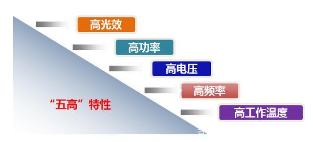 Five high characteristics of third-generation semiconductor materials
【one】
Three eras of semiconductor materials from the perspective of energy bands
The third-generation semiconductor materials are significantly superior to silicon (Si), germanium (Ge), and gallium arsenide (GaAs) in the fields of high-power, high-temperature, high-frequency, radiation-resistant microelectronics, and short-wavelength optoelectronics. properties of first- and second-generation semiconductor materials. The third-generation semiconductor materials are becoming the strategic commanding heights to seize the next-generation information technology, energy-saving emission reduction technology and national defense security technology, and are an important part of strategic emerging industries.
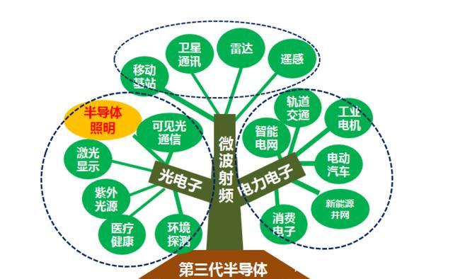 Third Generation Semiconductor Tree Diagram
From the perspective of energy band, it can also be divided into three semiconductor material eras.
The first generation of semiconductor materials is represented by elemental semiconductor materials such as silicon and germanium. Its typical application is integrated circuits, which are mainly used in low-voltage, low-frequency, low-power transistors and detectors. In the future, the dominant position of silicon semiconductor materials will still exist. However, the physical properties of silicon materials limit its application in optoelectronics and high-frequency electronic devices. For example, its indirect band gap determines that it cannot obtain high electro-optical conversion efficiency. And its narrow bandgap width (1.12 eV) and low saturation electron mobility (1450 cm2/V s) are not conducive to the development of high-frequency and high-power electronic devices.
The second-generation semiconductor materials are represented by gallium arsenide and indium phosphide (InP). The electron mobility of gallium arsenide material is 6 times that of silicon, and it has a direct band gap, so its device has high-frequency, high-speed photoelectric performance compared with silicon device, and it is recognized as a very suitable semiconductor material for communication. At the same time, its application in military electronic systems is increasingly extensive and irreplaceable. However, its forbidden band width range only covers 1.35 eV (InP) to 2.45 eV (AlP), which can only cover red light with a wavelength of 506 to 918 nm and light with longer wavelengths, and cannot meet the needs of short- and medium-wavelength optoelectronic devices. . Because the band gap of the second-generation semiconductor material is not large enough, the breakdown electric field is low, which greatly limits its application in the fields of high temperature, high frequency and high power devices. In addition, the toxicity of GaAs materials may cause environmental pollution problems and pose a potential threat to human health.
The third-generation semiconductor materials refer to group III nitrides (such as gallium nitride (GaN), aluminum nitride (AlN), etc.), silicon carbide, oxide semiconductors (such as zinc oxide (ZnO), gallium oxide (Ga2O3), calcium Titanium ore (CaTiO3), etc.) and diamond and other wide bandgap semiconductor materials. Compared with the previous two generations of semiconductor materials, the third-generation semiconductor materials have a large band gap, high breakdown electric field, high thermal conductivity, high electron saturation rate, and strong radiation resistance. Therefore, the third-generation semiconductor materials are used The prepared semiconductor devices can not only operate stably at higher temperatures, but also be more reliable under high voltage and high frequency conditions, and can also obtain higher operating capabilities with less power consumption.
【two】
Gallium Nitride (GaN) Material Development Potential
Gallium Nitride is a wide bandgap material that offers performance advantages similar to silicon carbide (SiC), but with greater potential for reduced cost. The industry believes that in the next few years, the cost of GaN power devices is expected to be reduced to the same price as silicon MOSFETs, IGBTs and rectifiers.
Gallium nitride power electronic devices have the advantages of higher operating voltage, higher switching frequency, and lower on-resistance, and are compatible with silicon-based semiconductor integrated circuit processes with extremely low cost and high technology maturity. It has great potential for development in the fields of a new generation of high-efficiency, small-sized power conversion and management systems, electric locomotives, and industrial motors.
The growing demand for high-speed, high-temperature, and high-power semiconductor devices has caused the semiconductor industry to reconsider the design and materials used in semiconductors. With the continuous emergence of a variety of faster and smaller computing devices, silicon materials have struggled to maintain Moore's Law. Due to the unique advantages of gallium nitride materials, such as excellent noise figure, high maximum current, high breakdown voltage, high oscillation frequency, etc., it provides a unique choice for a variety of applications, such as military, aerospace and defense, automotive fields, and High power fields such as industry, solar energy, power generation and wind power.
Due to the use of gallium nitride optoelectronic semiconductors in military, aerospace, national defense and consumer electronics, optoelectronic semiconductors have become the main product type in the global gallium nitride semiconductor device market and occupy an absolute dominant position. Among them, power semiconductor devices will become the fastest growing device in the future as the demand for high-power devices in industrial applications increases.
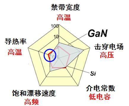 Gallium Nitride (GaN) Material Advantages
For the development of GaN power devices, market demand traction is crucial. From power supplies and PFC (power factor correction) (which will dominate the market in 2020), to UPS (uninterruptible power supply) and motor drives, many application areas will benefit from the characteristics of GaN-on-Si power devices.
Market research firm Yole Developpement believes that, in addition to these applications, pure electric vehicles (EV) and hybrid electric vehicles (HEV) will also begin to adopt these new materials and new devices after 2020. In terms of market size, the overall size of the GaN device market may reach approximately US$600 million in 2020. By then, a 6-inch wafer can process about 580,000 GaN. According to the assumption that EV and HEV adopt GaN from 2018 or 2019, the number of GaN devices will increase significantly from 2016 to 2020 at an average annual growth rate (CAGR) of 80%.
With the gradual maturity of 5G technology, it will bring business opportunities to the RF Front End (RF Front End) chip market, and the demand for RF Power Amplifiers (RF PA) will continue to grow in the future. Among them, the traditional metal oxide semiconductor (Laterally Diffused metal Oxide Semiconductor, LDMOS; LDMOS With the advantages of low cost and high power performance), the process is gradually replaced by Gallium Nitride (GaN), especially under the 5G technology that needs to support more components and higher frequencies, while Gallium Arsenide (GaAs) is relatively stable growth. Through the introduction of new radio frequency technology, RF PA will be realized with new process technology. Among them, GaN RF PA will become the mainstream process technology with output power above 3W, and the market share of LDMOS will gradually decrease.
Because 5G technology covers millimeter-wave frequencies and massive MIMO (Multi-Input Multi-Output) antenna applications to achieve 5G wireless integration and architectural breakthroughs, how to adopt Massive-MIMO and millimeter-wave (mmWave) backhaul systems on a large scale in the future will be is the key to development. Due to the high frequency of 5G, the demand for high-power, high-performance, and high-density radio frequency components has increased, among which gallium nitride (GaN) meets its conditions, that is, the GaN market has more potential business opportunities.
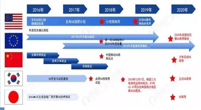 The promotion of 5G commercialization will accelerate the development of GaN RF market
【three】
What is Gallium Nitride (GAN)?
The research and application of GaN materials is the frontier and hot spot of global semiconductor research at present. It is a new semiconductor material for the development of microelectronic devices and optoelectronic devices. Together with semiconductor materials such as SIC and diamond, it is known as the successor to the first generation of Ge, Si Semiconductor materials, second-generation GaAs, and the third-generation semiconductor materials after InP compound semiconductor materials. It has properties such as wide direct band gap, strong atomic bond, high thermal conductivity, good chemical stability (hardly corroded by any acid) and strong radiation resistance. It is used in optoelectronics, high temperature and high power devices and high It has broad prospects in the application of high-frequency microwave devices.
Gallium nitride (GAN) is a typical representative of the third-generation semiconductor material, at T=300K, and is the core component of light-emitting diodes in semiconductor lighting. Gallium nitride is an artificial material. The conditions for the natural formation of gallium nitride are extremely harsh. It requires a high temperature of more than 2,000 degrees and a pressure of nearly 10,000 atmospheres to synthesize gallium nitride with metal gallium and nitrogen, which is impossible in nature. of.
Everyone knows that the first-generation semiconductor material is silicon, which mainly solves the problems of data calculation and storage; the second-generation semiconductor is represented by gallium arsenide, which is applied to optical fiber communication, and mainly solves the problem of data transmission; the third The next-generation semiconductor is represented by gallium nitride, which has outstanding performance in the conversion of electricity and light, and has higher efficiency in microwave signal transmission, so it can be widely used in various fields such as lighting, display, and communication. In 1998, American scientists developed the first gallium nitride transistor.
【Four】
Performance characteristics of gallium nitride (GAN)
High performance: mainly including high output power, high power density, high operating bandwidth, high efficiency, small size, light weight, etc. At present, the first-generation and second-generation semiconductor materials have reached the limit in terms of output power, and due to the advantages of GaN semiconductor in terms of thermal stability, it is easy to achieve high working pulse width and high working ratio, and the transmission at the antenna element level 10 times more power.
High reliability: The life of power devices is closely related to its temperature, the higher the temperature junction, the lower the life. GaN material has the characteristics of high temperature junction and high thermal conductivity, which greatly improves the adaptability and reliability of devices at different temperatures. GaN devices can be used in military equipment above 650°C.
Low cost: The application of GaN semiconductor can effectively improve the design of the transmitting antenna, reduce the number of transmitting components and the number of amplifier stages, etc., and effectively reduce the cost. At present, GaN has begun to replace GaAs as the T/R (receive/transmit) module electronic device material for new radars and jammers. The next-generation AMDR (solid-state active phased array radar) of the US military uses GaN semiconductors. The superior properties of gallium nitride, such as large band gap, high breakdown voltage, high thermal conductivity, high electron saturation drift speed, strong radiation resistance and good chemical stability, make it the highest electro-optic and photoelectric conversion efficiency in theory so far. It can become a key basic material for the preparation of wide-spectrum, high-power, high-efficiency microelectronics, power electronics, optoelectronics and other devices.
GaN's wide band gap (3.4eV) and sapphire and other materials are used as substrates, which have good heat dissipation performance and are conducive to the operation of devices under high-power conditions. With the continuous deepening of the research and development of III-nitride materials and devices, GaInN ultra-high blue and green LED technologies have been commercialized, and now major companies and research institutions in the world have invested heavily in the development of blue LEDs. of competition.
【five】
Gallium Nitride Applications
1. New electronic devices
The GaN material series has low heat generation rate and high breakdown electric field, and is an important material for the development of high-temperature, high-power electronic devices and high-frequency microwave devices. At present, with the progress of MBE technology in the application of GaN materials and the breakthrough of key thin film growth technology, various heterostructures of GaN have been successfully grown. New devices such as metal field effect transistor (MESFET), heterojunction field effect transistor (HFET) and modulation doped field effect transistor (MODFET) have been prepared with GaN materials. The modulated doped AlGaN/GaN structure has high electron mobility (2000cm2/v s), high saturation velocity (1×107cm/s), and low dielectric constant, and is a preferred material for making microwave devices; GaN Wide band gap (3.4eV) and sapphire and other materials are used as the substrate, which has good heat dissipation performance and is conducive to the operation of the device under high power conditions.
2. Optoelectronic devices
The GaN material series is an ideal short-wavelength light-emitting device material. The band gap of GaN and its alloys covers the spectral range from red to ultraviolet. Since Japan developed the homojunction GaN blue LED in 1991, InGaN/AlGaN double heterojunction ultra-brightness blue LED and InGaN single quantum well GaN LED have come out one after another. At present, Zcd and 6cd single quantum well GaN blue and green LEDs have entered the stage of mass production, thus filling the gap of blue LEDs in the market for many years. to shine
The development history of LED marked by efficiency is shown in Figure 3. Blue light-emitting devices have huge application markets in the fields of information access of high-density optical discs, all-optical displays, and laser printers. With the continuous deepening of the research and development of III-nitride materials and devices, GaInN ultra-high blue and green LED technologies have been commercialized, and now major companies and research institutions in the world have invested heavily in the development of blue LEDs. of competition.
In 1993, Nichia first developed a high-brightness GaInN/AlGaN heterojunction blue LED with a luminous brightness exceeding LCD, using Zn-doped GaInN as the active layer, with an external quantum efficiency of 2.7% and a peak wavelength of 450nm. change. In 1995, the company launched a commercial GaN green LED product with an optical output power of 2.0mW and a brightness of 6cd, with a peak wavelength of 525nm and a half-peak width of 40nm. Recently, using its blue LED and phosphorescence technologies, the company has launched white solid-state light-emitting device products with a color temperature of 6500K and an efficiency of 7.5 lumens/W. In addition to Nichia, companies such as HP and Cree have successively launched their own high-brightness blue LED products. The market for high-brightness LEDs is expected to jump from $386 million in 1998 to $1 billion in 2003. The applications of high-brightness LEDs mainly include automotive lighting, traffic signals and outdoor road signs, flat gold display, high-density DVD storage, blue-green light-to-submarine communication, etc.
After the successful development of Group III nitride blue LEDs, the focus of research began to shift to the development of Group III nitride blue LED devices. Blue LEDs have broad application prospects in the fields of light control measurement and high-density optical storage of information. At present, Nichia is a world leader in the field of GaN blue LEDs, and its GaN blue LEDs have a lifetime of more than 10,000 hours of continuous operation at 2mW at room temperature. Using sapphire as the substrate, HP has successfully developed the optical ridge waveguide refractive index-guided GaInN/AlGaN multi-quantum well blue LED. Cree Research was the first to report the CWRT blue laser made on SiC, which is a lateral device structure. Following companies such as Nichia, CreeResearch and Sony, Fujitsu announced the development of an InGaN blue laser, which can be used in CW at room temperature, its structure is grown on a SiC substrate, and a vertical conduction structure (P-type and n Contacts are made on the top and back of the wafer), which is the first reported CW blue laser with a vertical device structure.
In terms of detectors, a GaN ultraviolet detector has been developed with a wavelength of 369nm, and its response speed is comparable to that of Si detectors. But research in this area is still in its infancy. GaN detectors will have important applications in flame detection and missile early warning.
【six】
New infrastructure accelerates the development of gallium nitride
GaN wide bandgap power electronic devices represent the development direction of the field of power electronic devices. There are many problems to be solved in both materials and processes. Even if these problems are solved, their prices must still be more expensive than silicon-based. It is expected that by 2019, the price of GaN on silicon may drop to a level comparable to that of silicon materials. Because of their excellent characteristics, they may be mainly used in mid-to-high-end applications. Just as silicon fully-controlled devices cannot completely replace silicon half-controlled devices, SiC and GaN wide-bandgap power electronic devices are unlikely to completely replace silicon power MOSFETs and IGBTs in the future. and GTO (including IGCT). SiC power electronic devices will be mainly used in high-voltage industrial applications above 1200V; GaN power electronic devices will be mainly used in consumer electronics and computer/server power applications below 900V.
As a third-generation semiconductor material, GaN's properties determine that it will be more suitable for applications such as 4G and even future 5G technologies. Judging from the current market situation, GaAs is still the mainstream of mobile phone terminal PA and LNA, while LDMOS is in the dominance of base station RF. However, as Si materials and GaAs materials gradually reach their limits in performance, we expect that GaN semiconductors will be more and more used in the field of wireless communications.
The third-generation semiconductor radio frequency electronic devices have achieved large-scale applications in both civilian and military fields. In particular, due to the performance advantages of high frequency, high power, and large bandwidth, GaN radio frequency electronic devices and modules play an irreplaceable role in the construction of 5G mobile communication base stations. The acceleration of my country's 5G construction will trigger the development of GaN Rapid growth in demand for radio frequency electronics.
Jiangxi Yuhongjin Material Technology Co., Ltd. is committed to the development and production of third-generation semiconductors. Our company has a world-class scientific research team, advanced production equipment and national policy support. Our company will use advanced technology to try our best to bring you a better experience.
Building 7, Semiconductor Industrial Park, High-tech Zone, Fuzhou City, Jiangxi Province
www.yuhongjinchip.com
+86 198-8002-266
semiconductors
Next page
Next page
related News


Jiangxi Yuhongjin Material Technology Co., Ltd.
-
E-mail: steven@nitridesemi.com
-
Address: Building 6-7, Deke Industrial Park, Fuzhou High-tech Zone, Fuzhou City, Jiangxi Province

Powered by www.300.cn